

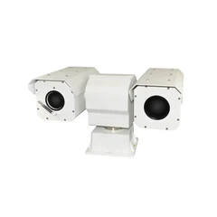
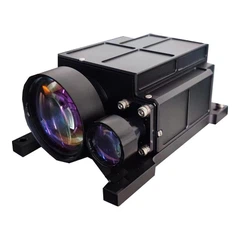
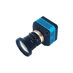

The resolution of the thermal sensor, specifically the microbolometer, serves as a crucial parameter in evaluating sensor quality. It denotes the number of sensitive elements (pixels) that form the sensor, and a higher pixel count in sensors contributes to the production of more detailed images of objects. Standard sizes for thermal imaging sensors are:
| Sensor resolution | Aspect ratio |
| 160x120 | 4:03 |
| 320x240 | 4:03 |
| 384x288 | 4:03 |
| 640x480 | 4:03 |
| 1024x768 | 4:03 |
Pixel Pitch and Thermal Imaging Sensor Measurements When delving into the complex technical specifications of digital image sensors, it's inevitable to come across a key metric called "pixel pitch." Essentially, pixel pitch is the width of a single pixel on a sensor, and is typically expressed in microns (μm). This simplifies the calculation of overall physical sensor size-just multiply the resolution by the pixel pitch. However, confusion arises when considering how these dimensions affect the field of view and level of detail of a thermal sensor. Unlike standard visible light sensors, where increasing resolution without changing sensor size can enhance image detail, thermal imagers follow a different paradigm. In thermal imaging, increasing resolution while maintaining pixel pitch can produce the same level of detail in the image, but with a wider field of view. With the context of pixel pitch differences, let's explore the difference between two common values: 17 microns and 12 microns. 17-micron pixel pitch: A pixel pitch of 17 microns means that the centers of adjacent pixels are 17 microns apart from each other. Sensors with this pixel pitch can be physically larger, which can offer benefits such as increased light sensitivity. In applications where greater sensitivity to infrared radiation is critical, a larger pitch is beneficial. 12-micron pixel pitch: On the other hand, a 12-micron pixel pitch means that the distance between the centers of the pixels is smaller. Sensors with a 12-micron pixel pitch are generally more compact, allowing for a higher pixel density within the same physical sensor size. This results in improved image resolution and finer detail, making them suitable for applications that require a high level of detail. At ATN, we address these distinctions by evaluating the effective detail of a camera using PPM (Pixels Per Millimeter). In addition, we use an in-house tool that allows us to preview the field of view for most sensor sizes at any focal length. For help selecting the best camera for your application and budget, contact us today. The special lens of a thermal imaging riflescope focuses the infrared light emitted by all objects within the field of view. The focused light is scanned by a phased array of infrared detector elements. The detector elements create a very detailed temperature pattern called a thermogram. It takes only about one-thirtieth of a second for the detector array to obtain the temperature information needed to make a thermogram. This information is obtained from thousands of points within the detector array's field of view. The thermogram created by the detector elements is converted into electrical pulses. These pulses are sent to the signal processing unit, a circuit board with a specialized chip that converts the information from the elements into data for display. The signal processing unit sends the information to the display, which displays various colors depending on the intensity of the infrared emission. All the pulses from all the elements are combined to form the image. Unlike traditional night vision devices that use image intensification technology, thermal imaging is ideal for detecting people or working in near-total darkness with little or no ambient light (such as stars, moonlight, etc.). ATN uses specially designed germanium-coated lenses for all thermal imaging products to increase the efficiency of the equipment.